
ISSN:
2181-3906
2024
International scientific journal
«MODERN
SCIENCE
АND RESEARCH»
VOLUME 3 / ISSUE 2 / UIF:8.2 / MODERNSCIENCE.UZ
74
ELECTRONIC SPECTROSCOPY OF HETEROSYSTEM SI/CU SURFACES
WITH NANOSCALE PHASES AND FILMS
A.A. Mustafoev
Jizzakh Polytechnic Institute.
https://doi.org/10.5281/zenodo.10629056
Abstract. In this article, valence electron state density, energy band parameters, energetic,
optical and electrophysical properties of metal oxide and silicide films with thickness ≤ 40 Å
formed on Si/Cu surface during ion implantation and annealing were studied.
Key words: thermal oxidation, nanophases, nanofilms, plasma oscillation, surface
roughness, optical-phonon mode, island growth.
ЭЛЕКТРОННАЯ СПЕКТРОСКОПИЯ ПОВЕРХНОСТЕЙ ГЕТЕРОСИСТЕМ
SI/CU С НАНОРАЗМЕРНЫМИ ФАЗАМИ И ПЛЕНКАМИ
Аннотация. В статье исследованы плотность состояний валентных электронов,
параметры энергетических зон, энергетические, оптические и электрофизические
свойства пленок оксидов металлов и силицидов толщиной ≤ 40 Å, образующихся на
поверхности Si/Cu в процессе ионной имплантации и отжига.
Ключевые слова: термическое окисление, нанофазы, нанопленки, плазменные
колебания, шероховатость поверхности, оптико-фононный режим, рост островков.
Introduction
Recently, nanoscale structures obtained on the surface and near it for materials of various
natures have been widely studied, which is due to their promise for the development of new POP
and MIS structures for solid-state electronics devices. Nanoscale systems can be obtained using
molecular beam, solid-phase and gas-phase epitaxy and ion bombardment methods. In this case,
it is of particular interest to obtain and study the properties of nanostructures based on freely
hanging films. Previously, the patterns of formation of nanosized films of SiO
2
and MeS
i2
(Me is
a metal) on the surface of a thin free-hanging Si/Cu heterostructure were studied. In particular, it
was found that the SiO
2
film obtained by ion bombardment followed by heating contains a large
amount of non-stoichiometric SiO
x
oxides and unbound Si atoms (5–6 at.%), and the BaSi2 and
CoSi
2
films contain excess metal atoms - up to 10 at. %. In this case, the Eg of the SiO
2
and BaSi
2
films decreased by more than two times [1-2].
In this dissertation, the densities of state of valence electrons, energy band parameters,
energetic, optical and electrophysical properties of metal oxide and silicide films with a thickness
of ≤ 40 Å formed on the Si/Cu surface during ion implantation followed by annealing were studied
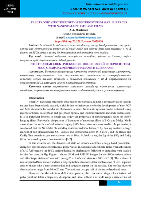
for the first time. In Fig. Figure 1. shows SEM and RHEED images for the Si/Cu surface before
and after implantation of ions with energy E = 1 keV and dose 6 × 10
15
sm
–2
[3]. The surface of
non-implanted Si is smooth and has a polycrystalline structure. After implantation of ions, separate
cluster phases with a new composition and structure appear on the surface. The surface sizes of
cluster phases range from 10 to 20 nm. These phases occupy half of the entire irradiated area.
However, in the electron diffraction pattern, the concentric rings characteristic of
polycrystalline films completely disappear, and new, diffuse and wide rings characteristic of

ISSN:
2181-3906
2024
International scientific journal
«MODERN
SCIENCE
АND RESEARCH»
VOLUME 3 / ISSUE 2 / UIF:8.2 / MODERNSCIENCE.UZ
75
disordered surfaces are observed. Apparently, it can be assumed that microstresses arising near the
cluster phases lead to disorder in non-irradiated areas of the surface. Starting from a dose D ≈ 2 ×
10
16
cm
–2
, overlapping boundaries of neighboring clusters are observed and, starting from a dose
of 10
17
sm
–2
, complete doping of the surface layers occurs and an amorphous layer of non-
stoichiometric silicon dioxide is formed - in the RHEED picture, instead of concentric rings, one
diffuse ring is observed – amorphous halo [4-5].
Fig. 1. SEM images and RHEED patterns (insets) for the Si/Cu(100) surface before (a)
and after (b) implantation with ions with energy E = 1.0 keV at a dose of 6 × 10
15
sm
–2
[3-4].
Experimental technique
After heating at a temperature of 750 K, the stoichiometric composition of the SiO
2
film
improves significantly (the SiO
2
concentration increases to 85–90 at.%), but the high degree of
amorphism remains.
The HPEE spectra of a free-hanging Si/Cu(100) structure before and after the formation of
a nano-sized oxide film are shown in Fig. 1. A number of intense peaks are detected in the Si/Cu
spectrum. The presence of peaks at energy values ΔE1 = 3.4, ΔE
2
= 6.7 and ΔE
4
= 14 eV can be
explained by the occurrence of interband transitions, and other peaks can be explained by the
excitation of surface (ΔE
3
= ħωs = 10.4, ΔE
6
= ħωs = 21 eV) and bulk (ΔE
5
= ħωv = 17 eV) plasma
oscillations [116; P. 102].
The spectrum of the SiO
2
nanofilm reveals two maxima due to interband transitions ΔE
1
=
9.1, ΔE
3
= 19 eV and two maxima due to plasma oscillations: ΔE
2
= ħωs = 15 and ΔE4 = ħωv =
23 eV. Note that the energy of plasma oscillations and interband transitions in a free SiO
2
/Si
nanofilm differs from the energy in the case of a thick SiO2 film.
Fig. 2. HPEE spectra of the Si/Cu(100) heterostructure before (1) and after (2) the
formation of the SiO2 film, Ep = 1000 eV [1-2].

ISSN:
2181-3906
2024
International scientific journal
«MODERN
SCIENCE
АND RESEARCH»
VOLUME 3 / ISSUE 2 / UIF:8.2 / MODERNSCIENCE.UZ
76
The nature of the shift of the maxima caused by interband electronic transitions is probably
associated with the deformation of the functions of electronic states with a decrease in the thickness
of the SiO2 film and an increase in the influence of the substrate.
When implanting barium with different doses after annealing, nanophases and layers of
barium silicides formed on the Si surface. Nanocluster phases and films (d=20-50 Å) of silicides
such as BaSi
2
and CoSi
2
were obtained.
Thus, after annealing freely hanging Si/Cu films implanted with O
2
+
and Ba
+
ions, three-
layer systems SiO
2
/Si/Cu and BaSi
2
/Si/Cu are formed [6-7].
In table Table 1 shows the band energy parameters, maximum values of the secondary
electron emission coefficient σm, quantum yield Y of photoelectrons, resistivity ρ of SiO
2
nanofilms and metal silicides. It can be seen that during the formation of metal silicides, the Eg
value of silicon decreases by three times, the resistivity by 10
4
times, the values of σm and Y by
one and a half to two times, and in the case of the formation of SiO
2
, E
g
increases by approximately
four times, ρ by 300 times, and σm and Y – two to three times [8-9].
Table 1
Zone parameters, σm, Y and resistivity (ρ) of the resulting films
Note: eϕ and Ф are thermionic and photoelectronic work functions.
However, these data differ markedly from the data for similar films obtained on the surface
of bulk Si films. For example, the Eg value for SiO2 and BaSi2 created on the surface of bulk Si
films is 7.9 and 0.7 eV, respectively. These differences are explained by the fact that in films of
SiO2 (as well as barium silicides) obtained on the surface of free films, due to the limitation of the
annealing temperature, they contain a certain amount of unbound atoms of silicon and oxide of the
SiOx type (1 ≤ x <2) [7-8].
REFERENCES
1.
K. Hoppe, W.R. Fahrner, D. Fink, S. Dhamodoran, A. Petrov, A. Chandra, A. Saad, F. Faupel,
V.S.K. Chakravadhanula, V. Zaporotchenko. Nucl. Instr. Meth. B., 266, 1642–1646 (2008).
2.
Д.Г. Громов, О.В. Пятилова, С.В. Булярский, А.Н. Белов, А.А. Раскин. ФТТ, 55(3), 562-
566 (2013).
Options
Si, d=400 Å
SiO
2
/Si, d=20 Å
BaSi
2
/Si,
d=50-60 Å
CoSi
2
/Si,
d= 50-60 Å
eφ, eV
5.1
3.9
3.1
-
Eg, eV
1.1
4.1
0.3
0.4
ρ,
μΩ cm
6
10
5
2
10
8
100-150
80-100
F, eV
5.2
4.9
3.9
4.1
χ
4.1
0.8
3.6
3.7
σm
1.2
2.2
2
1.7
Υ
8
10
-5
6
10
-4
4
10
-4
-

ISSN:
2181-3906
2024
International scientific journal
«MODERN
SCIENCE
АND RESEARCH»
VOLUME 3 / ISSUE 2 / UIF:8.2 / MODERNSCIENCE.UZ
77
3.
Y. Kanemitsu, T. Kushida. Appl. Phys. Lett., 77(22), 3550-3552 (2000).
4.
Z.A. Isakhanov, Z.E. Mukhtarov, B.E. Umirzakov, M.K. Ruzibaeva. Technical Physics,
56(4), 546-549 (2011).
5.
A.S. Rysbaev, Z.B. Khuzhaniyazov, A.M. Rakhimov, I.R. Bekpulatov. Technical Physics,
59(10), 1526-1530 (2014).
6.
Ю.К. Ундалов. ФТП, 49(7), 887-898 (2015).
7.
M. Hamasaki, T. Adachi, S. Wakayama, M. Kikuchi. J. Appl. Phys., 47(7), 3987-3992 (1978).
8.
О.Б. Гусев, А.Н. Поддубный, А.А. Прокофьев, И.Н. Яссиевич. ФТП, 47(2), 147-167
(2013).
9.
R Mirzaev, U., Abdullaev, E., Kholdarov, B., Mamatkulov, B., & Mustafoev, A. (2023).
Development of a mathematical model for the analysis of different load modes of operation
of induction motors. In E3S Web of Conferences (Vol. 461, p. 01075). EDP Sciences.
10.
Irisboyev, F. (2022). ELEKTR SIGNALLAR KUCHAYTIRGICHLARI VA ULARNING
ASOSIY PARAMETRLARI VA TAVSIFLARI. Евразийский журнал академических
исследований, 2(11), 190-193.
11.
Irisboyev,
F.
(2022).
YARIM
O‘TKAZGICHLI
MODDALARDAN
TAYYORLANADIGAN
KUCHAYTIRGICHLARNING
PARAMETRLARI
VA
XARAKTERISTIKALARI. Science and innovation, 1(A6), 374-377.
12.
Irisboyev, F. B. (2022). ELEKTRON ZANJIRLAR VA MIKROSXEMOTEXNIKA
QURILMALARINING ASOSLARI. Academic research in educational sciences, 3(10), 15-
19.
13.
Irisboyev, F. (2024). CLUSTERS OF SELENIUM ATOMS IN THE SILICON
LATTICE. Ilm-fan va ta'lim, 2(1 (16)).
14.
Irisboyev, F. (2024). ASYNCHRONOUS MACHINE TYPES, STRUCTURE AND
PRINCIPLE OF OPERATION. Ilm-fan va ta'lim, 2(1 (16)).
15.
Irisboyev, F. (2023). THE INPUTS ARE ON INSERTED SILICON NON-BALANCED
PROCESSES. Modern Science and Research, 2(10), 120-122.
16.
Boymirzayevich, I. F. (2023). THE INPUTS ARE ON INSERTED SILICON NON-
BALANCED PROCESSES.
17.
Irisboyev, F. (2022). PARAMETERS AND CHARACTERISTICS OF AMPLIFIERS MADE
OF SEMICONDUCTOR MATERIALS. Science and Innovation, 1(6), 374-377.